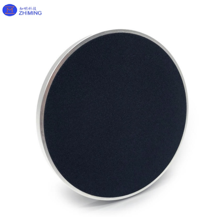
A Flip-Chip Bonding Vacuum Chuck is a high-precision vacuum adsorption component specifically designed for Flip-Chip Bonding processes in semiconductor manufacturing. Its core function is to stably adsorb and secure wafers or dies during bonding, ensuring micrometer or even sub-micrometer-level alignment and interconnection with the substrate. Typically fabricated from ultra-high-purity silicon (Si), silicon carbide (SiC), or specialty ceramics, it features internally precision-machined air channels and adsorption grooves. When connected to a negative pressure source, it generates a uniform negative pressure field, enabling non-contact or low-contact-stress adsorption of wafers to avoid damaging sensitive circuit patterns.
SiC Ceramic Vacuum Chuck Data
| Parameter Name | Typical Value/Range |
| Coefficient of Thermal Expansion | < 3.5 × 10⁻⁶/°C |
| Elastic Modulus | > 300 GPa |
| Bulk Density | > 3.1 g/cm³ |
| Surface Flatness | ≤ 1 μm |
| Surface Roughness (Ra) | ≤ 0.01 μm |
| Adsorption Groove Accuracy | ± 5 μm |
SiC Ceramic Vacuum Chuck Application Areas
- Flip-Chip Interconnection Processes: For precise alignment and bonding of high-end chips (e.g., CPUs, GPUs, FPGAs) to packaging substrates.
- Wafer-Level Packaging (WLP): Used in Fan-In and Fan-Out packaging to adsorb and secure wafers for bump formation, redistribution layer (RDL) patterning, and bonding.
- 2.5D/3D Integration: Enables precise pick-and-place and bonding of multiple dies during silicon interposer-based or chip-stacking processes.
- MEMS Packaging: Facilitates non-destructive handling and packaging of sensitive structures in microelectromechanical systems.
SiC Ceramic Vacuum Chuck Features

1. Precision Air Channel Machining: Utilizes micro-machining technologies (e.g., micro-milling, laser processing) to create complex and uniform air networks, ensuring highly consistent adsorption force distribution and preventing wafer warping or slippage.
2. Mirror Polishing: The working surface undergoes nanoscale polishing, achieving extremely low roughness (Ra ≤ 0.01μm), effectively reducing particulate contamination and electrostatic discharge (ESD) risks, and protecting wafer backside quality.
3. Ultra-Low Thermal Expansion Coefficient: The material’s CTE closely matches silicon wafers (typically < 4.5×10⁻⁶/℃), maintaining exceptional dimensional stability and alignment accuracy during thermal cycles (e.g., heating-bonding-cooling) in bonding processes.
4. High Stiffness: The material’s high elastic modulus (> 300 GPa) and optimized structural design minimize deformation under bonding pressure, ensuring chip coplanarity and uniform bonding.
5. High Density: The substrate exhibits very low porosity (typically < 0.5%), is non-porous, avoids gas retention and contaminant ingress, and meets the stringent requirements for ultra-high vacuum and cleanliness in semiconductor processes.
6. Exceptional Flatness and Parallelism: The overall flatness and parallelism to the mounting reference surface can reach within 1 micrometer (1μm), providing an absolute flat reference for chips, which is fundamental for ultra-precision bonding.
Recommended Customized SiC Ceramics
1. Customized SiC Boats Vertical & Horizontal Wafer Carriers
2. Customized SiC Ceramic Suction Cups for Lithography Applications

SiC Ceramic Vacuum Chuck FAQ
Q1: What is the primary function of a flip-chip bonding vacuum chuck?
A1: It is designed to stably adsorb and secure wafers or dies during flip-chip bonding processes, ensuring micrometer or sub-micrometer-level alignment between chips and substrates through vacuum force, which is critical for high-precision semiconductor packaging .
Q2: Why are materials like silicon carbide (SiC) preferred for flip-chip bonding vacuum chucks?
A2: Silicon carbide is chosen for its extremely low thermal expansion coefficient (~4.5×10⁻⁶/°C), high stiffness (>300 GPa), and exceptional chemical inertness, which ensure dimensional stability under high temperatures, prevent deformation during bonding, and resist corrosion from process gases like acids or plasmas .
Tags: # SiC Ceramic Vacuum Chuck, #Flip-Chip Bonding, #High-Purity, #Customized, #SiC Ceramics, #Mirror Polishing, #High-Stiffness